КАТЕГОРИИ:
Архитектура-(3434)Астрономия-(809)Биология-(7483)Биотехнологии-(1457)Военное дело-(14632)Высокие технологии-(1363)География-(913)Геология-(1438)Государство-(451)Демография-(1065)Дом-(47672)Журналистика и СМИ-(912)Изобретательство-(14524)Иностранные языки-(4268)Информатика-(17799)Искусство-(1338)История-(13644)Компьютеры-(11121)Косметика-(55)Кулинария-(373)Культура-(8427)Лингвистика-(374)Литература-(1642)Маркетинг-(23702)Математика-(16968)Машиностроение-(1700)Медицина-(12668)Менеджмент-(24684)Механика-(15423)Науковедение-(506)Образование-(11852)Охрана труда-(3308)Педагогика-(5571)Полиграфия-(1312)Политика-(7869)Право-(5454)Приборостроение-(1369)Программирование-(2801)Производство-(97182)Промышленность-(8706)Психология-(18388)Религия-(3217)Связь-(10668)Сельское хозяйство-(299)Социология-(6455)Спорт-(42831)Строительство-(4793)Торговля-(5050)Транспорт-(2929)Туризм-(1568)Физика-(3942)Философия-(17015)Финансы-(26596)Химия-(22929)Экология-(12095)Экономика-(9961)Электроника-(8441)Электротехника-(4623)Энергетика-(12629)Юриспруденция-(1492)Ядерная техника-(1748)
Calculations
|
|
|
|
There are two main categories of regulator, linear regulator and switching regulators. The simplest linear regulator uses a resistor and a Zener diode, as described earlier, but its performance is limited and most practical linear regulators use a transistor as a control element and an amplifier to provide an error signal within a negative feedback loop. The switching regulator incorporates a high – speed switching which is controlled by a feedback loop which monitors the output voltage. The switch produces a train of pulses whose duty ratio or frequency is controlled by the feedback loop. These pulses are averaged then to provide a DC output.
Because all mains – powered electronic equipment requires a voltage regulator, there are many linear and switching type regulators which are manufactured as integrated circuits and it is unlikely that a designer will be required to design a voltage regulator. Manufacturers’ application notes provide detailed design rules for each type and the purpose of this lectures is to provide an understanding of the operating principles to enable a sensible choice to be made.
Linear regulators
The linear voltage regulator uses a transistor to regulate the flow of current and the voltage supplied to the load from an unregulated source. The purpose of the regulator is to monitor the output voltage and, by means of feedback, to maintain it as constant as possible for all load currents. Transistors can be incorporated into a regulator either as a series control element or as a shunt element.
Series regulator
A simplified block diagram of series regulators is shown in the figure below.
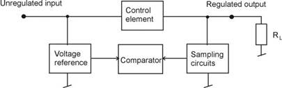
Control is achieved by comparing the required output with a fixed voltage reference. If the output voltage changes, for example as a result of a variation in the load current, the input to the comparator from the sampling circuit changes in the same direction. The output generated by the comparator, resulting from the error signal, causes the control element to vary the
output voltage in the opposite direction. This action continues until the comparator detects no difference between the reference voltage and the sampled voltage.
The figure below is a circuit diagram of a simple series regulator in which the control element is an npn bipolar transistor and a Zener diode acts as the voltage reference.
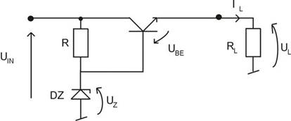
The comparator function is performed by the base emitter junction which controls current flow through the transistor.
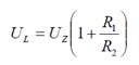
The output voltage is:
UL= UZ– UBE
If ULincreases then UBEdecreases and the transistor conducts less. The reduction in the load current will cause the voltage across the load to fall, which will restore the balance.
The voltage regulation is given by the same expression as or the simple Zener diode regulator:
However, the variation of the Zener current result from the variation of the base current which is times less than the possible change of the load current. The fact that the load current does not have to flow through R means that it can have a much larger value. Thus the regulation is greatly improved.
Further improvement in stability of the output voltage and more freedom in the choice of the Zener voltage is achieved by adding an op amp gain stage as shown in the following figure.
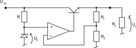
In this circuit the Zener voltage is more stable because the variation of the load current does not affect the Zener current. In addition, the large loop gain, resulting from the op amp, ensures that very small changes of the output voltage are detected ad rapidly corrected.
The output voltage settles to a value at which the input differential voltage of the op amp id almost zero so:
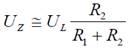
Then the output voltage is:
And it can be easily adjusted from a minimum value of UZby changing the resistor ratio.
The ripple rejection is improved by a factor 1+(kd0 ), where kd0is the open – loop gain of the amplifier and is the feedback factor,
 R 2 R 1 R 2
The output resistance is decreased by the same factor down to a few m, typically. Short – circuit protection
A serious limitation of the series regulator is that the transistor will be damaged if the output is short – circuited. Under short – circuit conditions the output current considerably increases (no feedback signal is applied to the op amp) and the full input voltage appears across the transistor. As a result the power dissipated in the transistor may increase tens of times in comparison with normal operating conditions, leading to the destimation of the transistor. Some means is thus required to limit the output short – circuit current.
A simple form of current limiter and the corresponding load current versus load voltage characteristic are shown below.
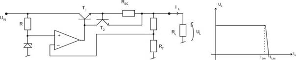
When UBE2= IL*RSCreaches UBEF= 0.7V T2begins to conduct heavily and consequently current which should be flowing into the base of T1is diverted to the collector of T2an thus T1is protected. The current through T2is limited by the current sourcing capability of the operational amplifier, which may be a few tens of mA.
Beyond
|

|
SC
the output voltage reduces to zero with only a relatively small additional increase in current. With this protection circuit the short – circuit power dissipation in the transistor is still a few times more than under normal operating condition so to ensure reliable operation the power rating for the transistor should correspond to the short – circuit conditions.
A further development of short – circuit protection is to reduce the current as well as the voltage when a short circuit occurs.
The idea of this type of current limiting, known as fold – back current limiting, is shown it the following figure.
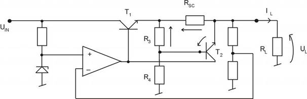
The circuit is similar to the basic, current – limiting circuit except that the base of T2is taken to a potential divider comprising R3and R4. The base – emitter voltage of T2 is:
UBE = UR3 - URSC
Under normal operating conditions URSCis smaller than UR3and the base – emitter junction of T2 is reverse – biased. As the load current increases the voltage drop across RSCincreases more rapidly than that across R3 until, at the maximum load current, the difference reaches UBEF= 0.7V.
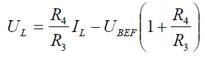
T2 begins to conduct and limits the current through T1. However, as the output voltage decreases the voltage across R3 decreases too and then a smaller value of URSC is required to maintain UBE at UBEF. The reduction of URSC is achieved by a reduction in the load current. The resulting graph of load current versus load voltage is shown below.
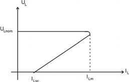
The maximum load current ILMis reached when the following condition is met:
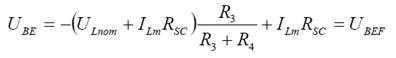
And from this point on the relationship between the output voltage and the load current is:
|
|

|
|
UBEF
⎜⎜1
⎝

|
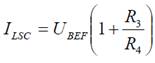
The short – circuit load current can be found by substituting UL=0 and then:
|
|
ILSC
UBEF
⎜⎜1
⎝
|
Thanks to a considerable decrease in the short – circuit load current the short – circuit power dissipation in T1may even be smaller than under normal operating conditions.
Shunt regulators
A block diagram of a shunt regulator is shown in the following figure.
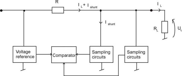
As for the series regulator the current through the control element is determined by the output voltage sample which is applied to the comparator.
However, instead of controlling the load current directly, the shunt regulator bypasses current to ground. The operation of the shunt regulator is similar to that of the simple Zener diode regulator; the current through the resistor R is approximately constant and the transistor controls the distribution of this current between itself and the load.
An example circuit diagram of a shunt regulator with an operational amplifier is shown below.
One important advantage of the shunt regulator is that it is not damaged by a short – circuited output. The short – circuit current is limited to UIN/R and provided the power rating for the resistor R is sufficient to withstand the short – circuit current, then there is no damage.
Integrated circuit regulators
For most applications it is not necessary to custom – design a voltage regulator, but rather to use any of the many “off – the – self” integrated circuit regulators.
The IC regulators are available as either fixed or adjustable regulators.
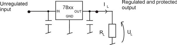
Typical of fixed voltage regulators are 78xx (positive output) and 79xx (negative output), where xx is the nominal output voltage and can be and of the following: 05, 06, 08, 10, 12, 15, 18 or 24.
The application of such fixed regulators is very simple and only requires connecting two additional capacitors of at least 100F directly to the input and toe output terminal, as shown in the figure.
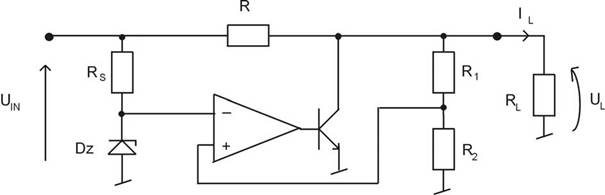
Adjustable regulators are used, for example, when a nonstandard regulated voltage is required. A simplified circuit diagram of a tree – terminal adjustable regulator (without protection circuits shown), of which LM317 is a classic representative, is shown below together with its application.

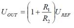
This regulator has no GROUND terminal. It adjust UOUTto maintain a constant voltage of UREF (UREF= 1.25 for LM317) between the output terminal and the adjustment terminal.
It can be easily shown that the output voltage is:
When choosing an IC voltage regulator for a specific application the following parameters should be considered (the values in brackets are typical):
- output voltage and its tolerance (1-2%)
- minimum dropout voltage (the minimum voltage drop must be maintained between the input and the output)(0.5 – 2V)
- maximum input voltage (35 – 40V)
- maximum output current (0.1A – 5A)
- ripple rejection = 20log Uripple(in)/Uripple(out) (60 – 80db)
- load regulation =(ULno load – UL full load)/ UL no load (0.1 – 0.5%)
- line regulation (DC input rejection) =UL/ULnomfor a given Uin(0.1 – 0.2%)
- temperature stability =UL/ULnomfor a given T, for example 0 – 100oC
- output impedance (0.01 – 0.1at low frequency of variable load current, for example 10Hz, increases with frequency).
|
|
|
|
|
Дата добавления: 2015-08-31; Просмотров: 342; Нарушение авторских прав?; Мы поможем в написании вашей работы!