КАТЕГОРИИ:
Архитектура-(3434)Астрономия-(809)Биология-(7483)Биотехнологии-(1457)Военное дело-(14632)Высокие технологии-(1363)География-(913)Геология-(1438)Государство-(451)Демография-(1065)Дом-(47672)Журналистика и СМИ-(912)Изобретательство-(14524)Иностранные языки-(4268)Информатика-(17799)Искусство-(1338)История-(13644)Компьютеры-(11121)Косметика-(55)Кулинария-(373)Культура-(8427)Лингвистика-(374)Литература-(1642)Маркетинг-(23702)Математика-(16968)Машиностроение-(1700)Медицина-(12668)Менеджмент-(24684)Механика-(15423)Науковедение-(506)Образование-(11852)Охрана труда-(3308)Педагогика-(5571)Полиграфия-(1312)Политика-(7869)Право-(5454)Приборостроение-(1369)Программирование-(2801)Производство-(97182)Промышленность-(8706)Психология-(18388)Религия-(3217)Связь-(10668)Сельское хозяйство-(299)Социология-(6455)Спорт-(42831)Строительство-(4793)Торговля-(5050)Транспорт-(2929)Туризм-(1568)Физика-(3942)Философия-(17015)Финансы-(26596)Химия-(22929)Экология-(12095)Экономика-(9961)Электроника-(8441)Электротехника-(4623)Энергетика-(12629)Юриспруденция-(1492)Ядерная техника-(1748)
Reading. 1.Listen to the text and answer the questions below
|
|
|
|
Warm up
1. Listen to the text and answer the questions below.
Have you ever heard of a 1940s computer called the ENIAC? It was about the same length and weight as three to four double-decker buses and contained 18,000 buzzing electronic switches known as vacuum tubes. Despite its gargantuan size, it was thousands of times less powerful than a modern laptop – a machine about 100 times smaller.
If the history of computing sounds like a magic trick – squeezing more and more power into less and less space – it is! What made it possible was the invention of the integrated circuit (IC) in 1958. It's a neat way of cramming hundreds, thousands, millions, or even billions of electronic components onto tiny chips of silicon no bigger than a fingernail. Let's take a closer look at ICs and how they work!
1) What was the ENIAC?
2) When was the ENIAC used?
3) What was the ENIAC’s size?
4) How many vacuum tubes did the ENIAC contain?
5) What invention made it possible to squeeze more power into less space? When was it?
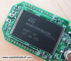
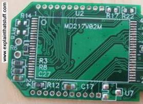
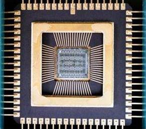
2. Match the descriptions 1-3 with the photos a-c in Fig. 4.2. Put the descriptions in logical order. Give names to the photos a-c in Fig. 4.2.
 a)
a)  b)
b)
 c)
c)
Fig. 4.2 Photo by courtesy of NASA Glenn Researech Center (NASA-GLC).
1) A traditional printed circuit board (PCB) like this has tracks linking together the terminals (metal connecting legs) from different electronic components. Think of the tracks as "streets" making paths between "buildings" where useful things are done (the components themselves). There's a miniaturized version of a circuit board inside an integrated circuit: the tracks are created in microscopic form on the surface of a silicon wafer.
2) If you could lift the cover off a typical microchip, this is what you'd find inside. The integrated circuit is the tiny square in the center. Connections run out from it to the terminals (metal pins or legs) around the edge. When you hook up something to one of these terminals, you're actually connecting into the circuit itself. You can just see the pattern of electronic components on the surface of the chip itself.
3) This is what an IC looks like when it's conveniently packaged inside a flash memory chip. Inside the black protective case, there's a tiny integrated circuit, with millions of transistors capable of storing millions of binary digits of information.
|
|
|
|
|
Дата добавления: 2014-11-29; Просмотров: 1235; Нарушение авторских прав?; Мы поможем в написании вашей работы!